- 您现在的位置:买卖IC网 > Sheet目录332 > IRS2109SPBF (International Rectifier)IC HALF BRIDGE DRIVER 8-SOIC
IRS2109/IRS21094(S)PbF
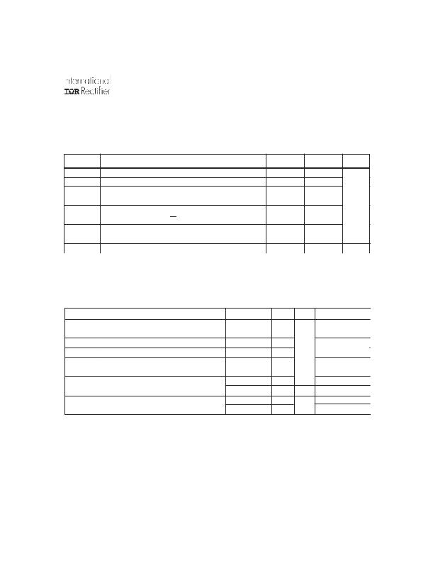
Recommended Operating Conditions
The input/output logic timing diagram is shown in Fig . 1. For proper operation the device should be used within the
recommended conditions. The V S and V SS offset rating are tested with all supplies biased at a 15 V differential.
Symbol
VB
V S
V HO
V CC
V LO
V IN
DT
V SS
T A
Definition
High-side floating supply absolute voltage
High-side floating supply offset voltage
High-side floating output voltage
Low-side and logic fixed supply voltage
Low-side output voltage
Logic input voltage (IN & SD)
Programmable deadtime pin voltage (IRS21094 only)
Logic ground (IRS21094 only)
Ambient temperature
Min.
V S + 10
(Note 1)
V S
10
0
V SS
V S S
-5
-40
Max.
V S + 20
600
V B
20
V CC
V CC
V CC
5
125
Units
V
° C
Note 1: Logic operational for V S of -5 V to +600 V. Logic state held for V S of -5 V to -V BS . (Please refer to the Design Tip
DT97-3 for more details).
Dynamic Electrical Characteristics
V BIAS (V CC , V BS ) = 15 V, V SS = COM, C L = 1000 pF, T A = 25 ° C, DT = V SS unless otherwise specified.
Symbol
Definition
Min.
Typ.
Max. Units Test Conditions
ton
toff
tsd
MT
tr
tf
Turn-on propagation delay
Turn-off propagation delay
Shutdown propagation delay
Delay matching, HS & LS turn-on/off
Turn-on rise time
Turn-off fall time
—
—
—
—
—
—
750
200
2 00
0
100
35
950
280
280
70
220
80
ns
V S = 0 V
V S = 0 V or 600 V
V S = 0 V
DT
MDT
Deadtime: LO turn-off to HO turn-on(DT LO-HO ) &
HO turn-off to LO turn-on ( DT HO-LO )
Deadtime matching = DT LO - HO - DT HO-LO
400
4
—
—
540
5
0
0
680
6
60
600
μ s
ns
R DT = 0 ?
R DT = 200 k ? (IR21094)
R DT = 0 ?
R DT = 200 k ? (IR21094)
www.irf.com
3
发布紧急采购,3分钟左右您将得到回复。
相关PDF资料
IRS2111PBF
IC DRIVER HALF-BRIDGE 8-DIP
IRS2112SPBF
IC DRIVER HI/LOW SIDE 16-SOIC
IRS2113MPBF
IC DRIVER HIGH/LOW SIDE 16MLPQ
IRS2113SPBF
IC DRIVER HIGH/LOW SIDE 16-SOIC
IRS2117PBF
IC DRIVER MOSFET/IGBT 1CH 8-DIP
IRS2124STRPBF
IC DVR HI SIDE 600V 500MA 8-SOIC
IRS21271STRPBF
IC DVR CURRENT SENSE 1CH 8-SOIC
IRS21531DSTRPBF
IC DRVR SELF-OSC HALF BRG 8-SOIC
相关代理商/技术参数
IRS2109SPBF
制造商:International Rectifier 功能描述:IC MOSFET DRIVER HALF-BRIDGE 8SOIC 制造商:International Rectifier 功能描述:IC, MOSFET DRIVER HALF-BRIDGE 8SOIC 制造商:International Rectifier 功能描述:IC, MOSFET DRIVER HALF-BRIDGE 8SOIC; Device Type:MOSFET; Module Configuration:High Side; Peak Output Current:600mA; Supply Voltage Min:10V; Supply Voltage Max:20V; Driver Case Style:SOIC; No. of Pins:8; Input Delay:750ns; Output ;RoHS Compliant: Yes
IRS2109STRPBF
功能描述:功率驱动器IC Hlf Brdg Drvr Soft Trn On Sngl 540ns RoHS:否 制造商:Micrel 产品:MOSFET Gate Drivers 类型:Low Cost High or Low Side MOSFET Driver 上升时间: 下降时间: 电源电压-最大:30 V 电源电压-最小:2.75 V 电源电流: 最大功率耗散: 最大工作温度:+ 85 C 安装风格:SMD/SMT 封装 / 箱体:SOIC-8 封装:Tube
IRS2110
制造商:IRF 制造商全称:International Rectifier 功能描述:HIGH AND LOW SIDE DRIVER
IRS2110-1PBF
制造商:International Rectifier 功能描述:IC DRIVER HIGH/LOW SIDE DIP14
IRS2110-2PBF
制造商:International Rectifier 功能描述:IC HIGH/LOW SIDE DRIVER DIP16
IRS2110PBF
功能描述:功率驱动器IC Hi&Lw Sd Drvr All HiVolt Pins 1 Sd RoHS:否 制造商:Micrel 产品:MOSFET Gate Drivers 类型:Low Cost High or Low Side MOSFET Driver 上升时间: 下降时间: 电源电压-最大:30 V 电源电压-最小:2.75 V 电源电流: 最大功率耗散: 最大工作温度:+ 85 C 安装风格:SMD/SMT 封装 / 箱体:SOIC-8 封装:Tube
IRS2110SPBF
功能描述:功率驱动器IC HI LO SIDE DRVR 600V 2A 120ns RoHS:否 制造商:Micrel 产品:MOSFET Gate Drivers 类型:Low Cost High or Low Side MOSFET Driver 上升时间: 下降时间: 电源电压-最大:30 V 电源电压-最小:2.75 V 电源电流: 最大功率耗散: 最大工作温度:+ 85 C 安装风格:SMD/SMT 封装 / 箱体:SOIC-8 封装:Tube
IRS2110STRPBF
功能描述:功率驱动器IC Hi&Lw Sd Drvr All HiVolt Pins 1 Sd RoHS:否 制造商:Micrel 产品:MOSFET Gate Drivers 类型:Low Cost High or Low Side MOSFET Driver 上升时间: 下降时间: 电源电压-最大:30 V 电源电压-最小:2.75 V 电源电流: 最大功率耗散: 最大工作温度:+ 85 C 安装风格:SMD/SMT 封装 / 箱体:SOIC-8 封装:Tube
